What did SemiAnalysis report about Nvidia's Kyber NVL144?
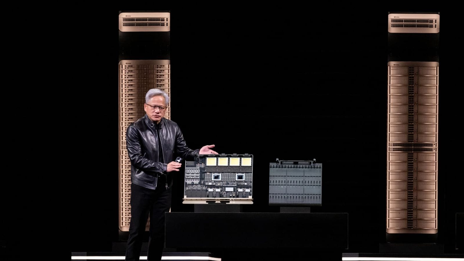
On July 6, 2026, semiconductor research firm SemiAnalysis posted six consecutive tweets on X revealing that Nvidia's Kyber NVL144 rack architecture is delayed by more than 12 months, pushing it to 2028. The firm stated: "Major delay: Just three months after Jensen Huang showcased the Kyber NVL144 at GTC, the product has suffered a major setback, with delays exceeding 12 months, pushing its launch to 2028."
The news drew market attention in pre-market trading, according to moomoo.com's coverage of the SemiAnalysis report.
Why is the Kyber NVL144 delayed?
The direct cause is a single hardware component: the midplane PCB, which Nvidia officially calls the "orthogonal backplane." This board enables 90-degree vertical interconnects between compute trays and switch trays inside the Rubin Ultra cabinet. It eliminates traditional cable runs by connecting trays board-to-board.
Manufacturing it is the problem. The backplane uses a hybrid of M9-grade copper-clad laminate, quartz fabric, and PTFE. It has 78 layers — formed by laminating three 26-layer boards together — with trace widths and spacings of 25 micrometers or less. That level of precision is required to meet SerDes signal integrity at rates exceeding 448G.
SemiAnalysis noted that connecting 144 GPUs in a single domain via copper cabling would require over 20,000 cables and add more than 30% weight. The orthogonal backplane is described as one of the few viable alternatives under current technology.
What happened to the NVL72x2 backup plan?
Nvidia had developed a fallback: the NVL72x2 back-to-back rack architecture. The design placed two Oberon racks back-to-back and used pure copper NVLink to scale the domain, bypassing the midplane PCB problem entirely.
You might also like
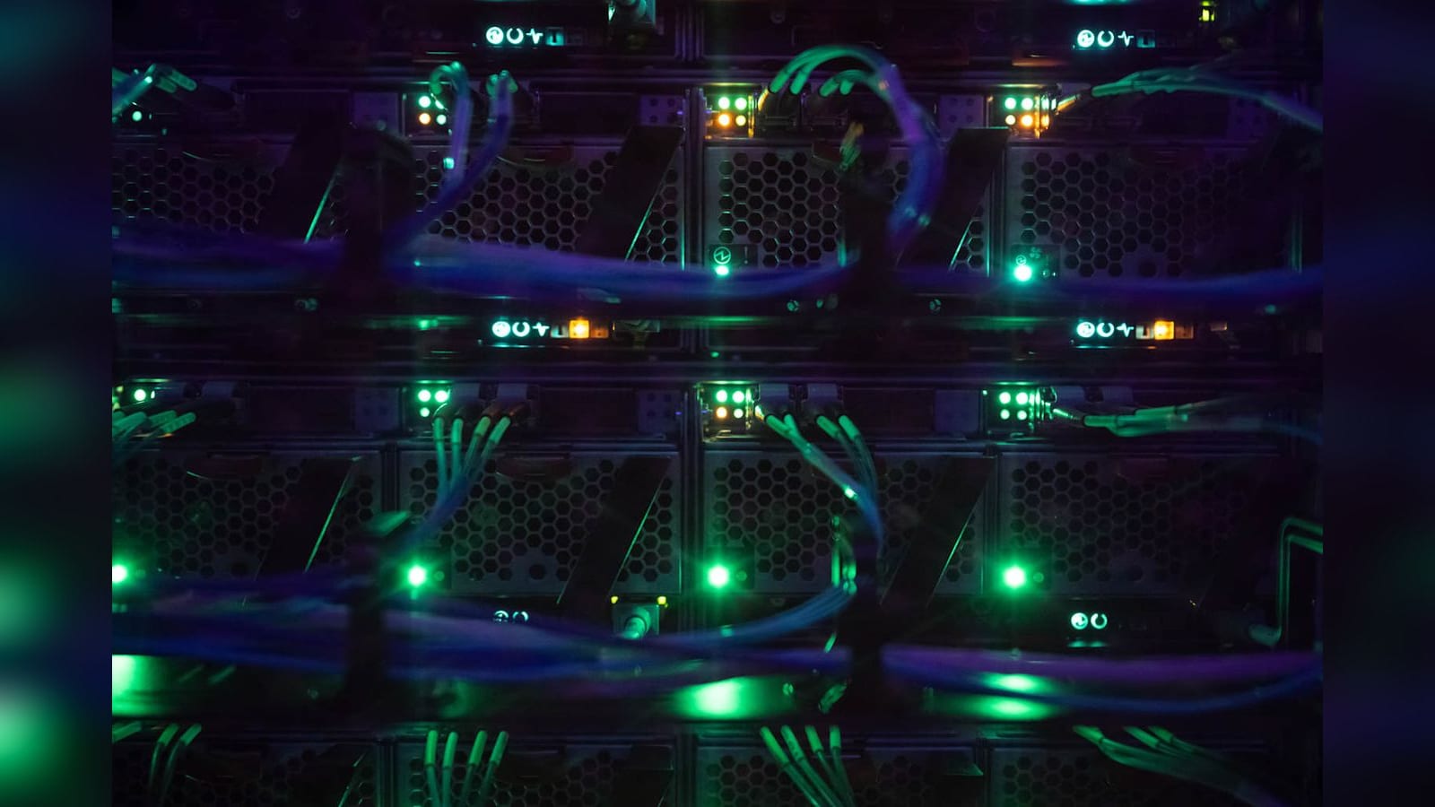



That plan is also gone. SemiAnalysis said the NVL72x2 was canceled "due to strong objections from cloud service providers and hyperscale data center operators over its unconventional design and heavy operational burden." With both paths blocked, Nvidia currently has no proven solution for scaling the Rubin Ultra domain.
Is the four-die Rubin Ultra GPU also canceled?
Yes, according to SemiAnalysis. The originally planned four-die Rubin Ultra — which would have used four compute chiplets and 16 HBM4E stacks for 1 TB of memory per package — has been scrapped. The reason cited is "manufacturing execution concerns."
Tom's Hardware reported on June 30, 2026 that connecting four near reticle-sized dies using existing advanced packaging technologies is a major engineering challenge. Cooling four complex dies alongside 16 HBM4E modules adds further cost and complexity.
Here's what the two designs look like side by side, based on what the sources report:
| Specification | Original Rubin Ultra | Reported New Direction |
|---|---|---|
| Compute dies | 4 | 2 |
| HBM4E stacks | 16 | 8 |
| Memory per package | 1 TB | Lower (unconfirmed) |
| Primary concern | Maximum density | Better manufacturability |
| Status | Canceled (per SemiAnalysis) | Not officially confirmed |
SemiAnalysis said the two-die Rubin Ultra delivers "approximately half" the performance of the four-die version. Nvidia has not officially confirmed the change.
How does Nvidia plan to compensate for lower per-package performance?
SemiAnalysis said Nvidia will respond by "significantly increasing sales of Oberon Rubin racks and Oberon Rubin Ultra racks." The logic is more units at the rack level to offset reduced per-package compute.
Here's what we know so far: none of this is officially confirmed by Nvidia. The source chain is SemiAnalysis via X, picked up by Tom's Hardware and igorslab.de — credible, but not an official Nvidia specification.
What is the status of the NVL576?
The NVL576 — a larger system connecting eight Oberon racks via CPO (Co-Packaged Optics) between NVSwitches — is also under pressure. SemiAnalysis said it "may also face delays or be limited to low-volume shipments given the current challenges facing CPO."
CPO is an optical interconnect technology Nvidia is introducing at scale for the first time in the Rubin Ultra generation. SemiAnalysis noted that a CPO NVSwitch is not expected to be fully production-ready until the next-generation Feynman platform.
Which competitors could benefit?
SemiAnalysis stated directly: "Nvidia currently has no proven solution to scale the Rubin Ultra scale-up domain, which leaves room for competitors such as AMD MI500X or TPUv8i Broadfly to surpass Rubin Ultra in scale-up capability."
The gap exists specifically in large-scale training scenarios where domain size matters. Nvidia's own roadmap places a working CPO NVSwitch in the Feynman generation, not Rubin Ultra.
What does this mean for the supply chain?
SemiAnalysis flagged that these delays and cancellations affect memory, PCB, and ODM supply chains. The 78-layer midplane PCB represents the current limit of high-end PCB manufacturing. A reduced HBM4E configuration — eight stacks instead of sixteen — changes demand forecasts for SK Hynix, Samsung, and Micron, who plan HBM capacity long in advance. The AI memory chip shortage dynamic makes those shifts significant.
For context on how advanced packaging constraints are shaping AI hardware decisions, see our coverage of Intel EMIB packaging and Micron's HBM expansion. The broader trend of hyperscalers building their own silicon — covered in our piece on Amazon custom chips — is part of the same pressure on Nvidia's roadmap.
SemiAnalysis confirmed that Nvidia's Rubin-based products are still expected to become available through partners in the second half of 2026 — but that refers to the standard Rubin platform, not Rubin Ultra or the Kyber rack.

0 Comments
Log in to comment
Not a member yet? Join the community
Pick a meme
KlipyHave a great take?
Drop your email — we'll send a magic link so you can post it. No password.
Not a member of the community? Join today.
Join the community →