
What is Intel EMIB and why does it matter for AI chips?
EMIB is Intel's Embedded Multi-die Interconnect Bridge, a packaging technology that connects multiple chips inside a single package. It is now being evaluated as an alternative to TSMC's dominant CoWoS packaging for Nvidia's next-generation chip architecture, according to reporting from Damn Ang's Substack.
In March 2026, Intel CFO David Zinsner told the Morgan Stanley conference that the packaging business was shaping up to be significantly larger than originally anticipated.
Why has advanced packaging become so critical?
The semiconductor industry's bottleneck has shifted. For a long time, performance gains came from shrinking transistors. That's no longer the whole story.
Today, what matters is how fast and efficiently you can connect multiple chips inside a single package. As chipstrat.com explains, the packaging itself is now becoming the dominant cost variable in the bill of materials for AI accelerators.
The root cause is the reticle limit: the largest area a lithography stepper can pattern in a single exposure, roughly 26 mm × 33 mm, or about 858 mm². Nvidia's H100 was already pushing that ceiling. Blackwell broke through it by stitching two reticle-sized compute dies together. Once you need more than one die, you need advanced packaging.
This pressure on AI memory chip supply chains extends well beyond wafers and transistors.
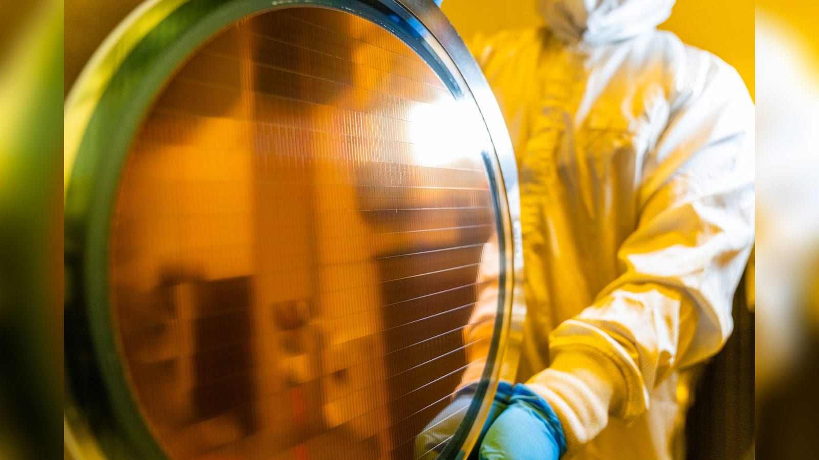
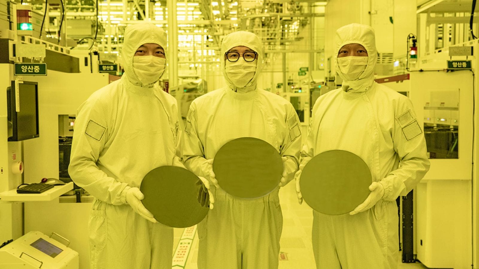
What is TSMC's CoWoS and why is supply tight?
CoWoS (Chip on Wafer on Substrate) is TSMC's family of advanced packaging technologies. It is the dominant method for packaging high-performance AI chips today. Nvidia's AI GPUs, AMD's accelerators, and Broadcom's custom ASICs are all packaged using CoWoS.
You might also like
The problem is supply. By industry estimates, Nvidia absorbs a substantial portion of available CoWoS capacity, leaving other customers struggling to secure allocation.
CoWoS comes in several variants — CoWoS-S, CoWoS-R, and CoWoS-L. Chipstrat also notes chatter about TSMC leaning on panel-level packaging (CoPoS) to handle Nvidia's Rubin Ultra, which allegedly requires four reticle-sized compute dies stitched together into one package. There are also reported rumors of a warpage problem on that four-die package, with a possible fallback to a 2+2 configuration.
How does Intel EMIB compare to TSMC CoWoS?
Here's what we know so far from the sources on the two approaches:
| Feature | TSMC CoWoS | Intel EMIB |
|---|---|---|
| Current AI chip customers | Nvidia, AMD, Broadcom | Being evaluated for Nvidia next-gen |
| Supply status | Constrained; Nvidia absorbs large share | Described as significantly larger opportunity than anticipated |
| Packaging family variants | CoWoS-S, CoWoS-R, CoWoS-L, CoPoS | EMIB (Embedded Multi-die Interconnect Bridge) |
| Industry position | Dominant | Challenger |
Intel CFO David Zinsner's March 2026 comments at the Morgan Stanley conference were the clearest public signal yet that Intel Foundry sees packaging as a major revenue opportunity.
What is Nvidia's Rubin Ultra and why does it stress packaging?
Nvidia's Rubin Ultra is reportedly a chip so large it requires four reticle-sized compute dies stitched together into one package. That scale makes the packaging architecture a central engineering and cost challenge, not just a manufacturing detail.
The reported warpage problem on the four-die package illustrates how difficult this gets at scale. TSMC is said to be exploring CoPoS (panel-level packaging) as one potential solution, with a 2+2 die configuration as a possible fallback.
Nvidia's need for packaging capacity at this scale is part of what opens the door for Intel EMIB as an alternative supplier. The Taiwan Super Micro supply chain story shows how tightly Nvidia's hardware ecosystem is scrutinized.
Why are materials also becoming a bottleneck?
Packaging is not the only constraint. SemiAnalysis noted on Threads that one of the most underappreciated angles on the AI semiconductor buildout is materials — not just chips or fab equipment, but the critical materials that make modern chips possible.
A separate thread flagged China's indium phosphide controls as a hidden materials story inside AI infrastructure. AI data centers increasingly depend on compound semiconductors inside optical interconnects. The data center optics supply chain is one area where materials constraints are already visible.
Applied Materials also unveiled new 3D chipmaking and hybrid bonding systems aimed at scaling AI hardware, with executives from Nvidia, Intel, and Samsung focusing on advanced packaging — chiplets and 3D stacking — as the next performance lever at a VLSI panel.
This materials pressure connects to broader AI memory supercycle dynamics that are reshaping semiconductor supply chains through the end of the decade.
What does this mean for Intel Foundry?
Intel Foundry has struggled to compete with TSMC on leading-edge logic. Packaging is a different competitive axis — and one where Intel has existing technology in EMIB.
Multiple outlets reported that Intel's EMIB was being evaluated for Nvidia's next-generation architecture. Intel CFO David Zinsner's March 2026 statement at the Morgan Stanley conference — that the packaging business was shaping up to be significantly larger than originally anticipated — is the most concrete public signal of that opportunity.
The IBM nanostack work on chip density shows that multiple companies are pursuing different paths to push beyond the reticle limit.
The confirmed next milestone: Intel's packaging business trajectory, as described by CFO David Zinsner at the Morgan Stanley conference in March 2026, with Nvidia's next-generation architecture evaluation still ongoing.


0 Comments
Log in to comment
Not a member yet? Join the community
Pick a meme
KlipyHave a great take?
Drop your email — we'll send a magic link so you can post it. No password.
Not a member of the community? Join today.
Join the community →