What did IBM announce on June 25, 2026?
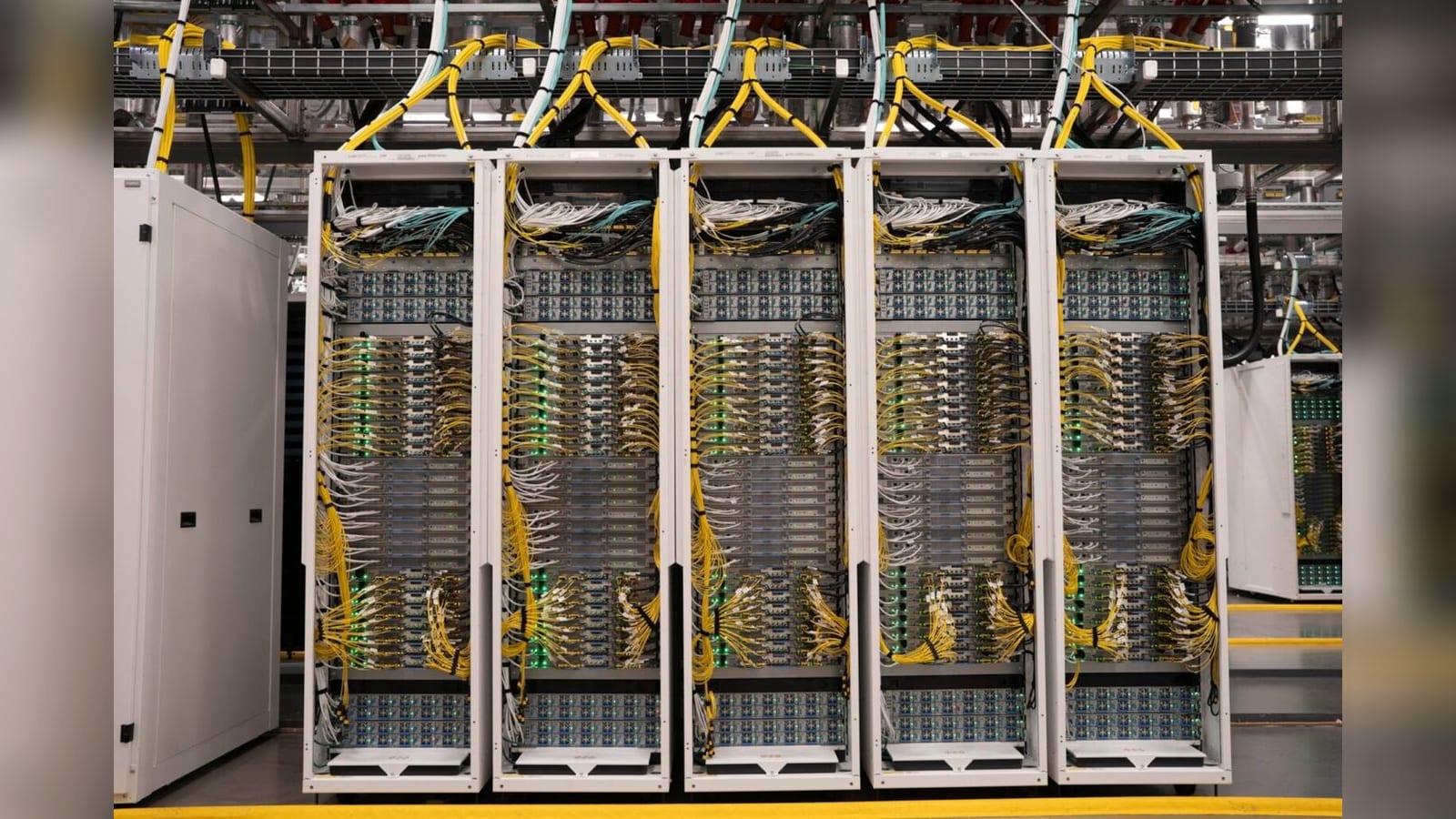
IBM unveiled a sub-1 nanometer chip design called Nanostack on June 25, 2026. The design packs roughly 100 billion transistors onto a fingernail-sized chip — nearly double the density of today's leading 2nm chips. IBM says the new architecture can deliver up to 50% more computing performance and 70% better energy efficiency.
IBM VP Huiming Bu, who leads chip research and development, put it plainly in a briefing with reporters: "Everyone demands more performance, but no one wants to pay for the power."
How does IBM's Nanostack technology work?
Historically, chipmakers improved performance by shrinking transistors horizontally across a flat silicon surface. That approach has largely hit its physical limits — components are already only a few atoms wide.
IBM's answer is 3D Sequential Integration, the technique behind Nanostack. Instead of placing transistors side by side, IBM stacks them vertically. That vertical stacking is what allows a single chip to house approximately 100 billion transistors, compared to roughly 50 billion on current leading-edge designs.
The architecture also improves SRAM scaling by 40%, according to IBM. That lets processors keep more data close to computing cores, reducing bottlenecks in tasks like text generation and image processing.
Note that "0.7nm" is not a literal measurement of transistor size. As 24/7 Wall St. via Yahoo Finance reports, modern process node labels are largely marketing terms representing advances in architecture and density, not physical dimensions.
You might also like


How does Nanostack compare to current chips?
Here's what the sources report on the key metrics:
| Metric | Current Leading-Edge Chips | IBM 0.7nm Nanostack |
|---|---|---|
| Transistor Density | ~50 billion | ~100 billion |
| Performance Gain | Baseline | Up to 50% higher |
| Power Consumption | Baseline | Up to 70% lower |
| AI Processing Power | Baseline | Up to 7,000 TOPS |
IBM estimates a specialized AI accelerator built on this architecture could deliver up to 7,000 trillion operations per second (TOPS). That is roughly seven times the capability of current AI hardware, according to 24/7 Wall St.
Why does this matter for AI data centers?
Power is a severe constraint for AI infrastructure. As The New York Times reports, energy-hungry AI chips have in some cases caused construction delays for data center builders who cannot secure affordable electricity.
IBM's design gives data center operators a choice:
- Up to 50% more performance at existing power levels
- Up to 70% less power consumption at existing performance levels
Both options address real bottlenecks in AI infrastructure today. The AI memory supercycle and the broader push for denser, more efficient compute are directly tied to these kinds of architectural advances.
Is IBM becoming a chip manufacturer?
No. IBM sold its commercial semiconductor manufacturing business to GlobalFoundries in 2014. It now operates as a semiconductor research organization, developing chip architectures and licensing the intellectual property to manufacturing partners.
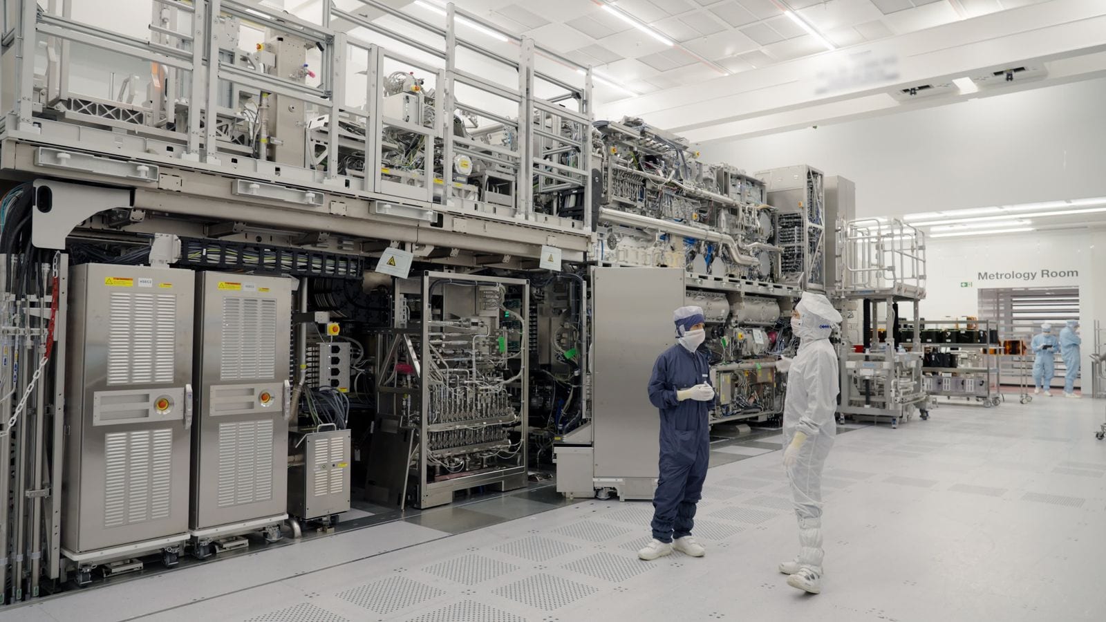
IBM's Albany, NY research center is where this work happens. The company avoids spending tens of billions of dollars on fabrication plants while still shaping the industry's direction.
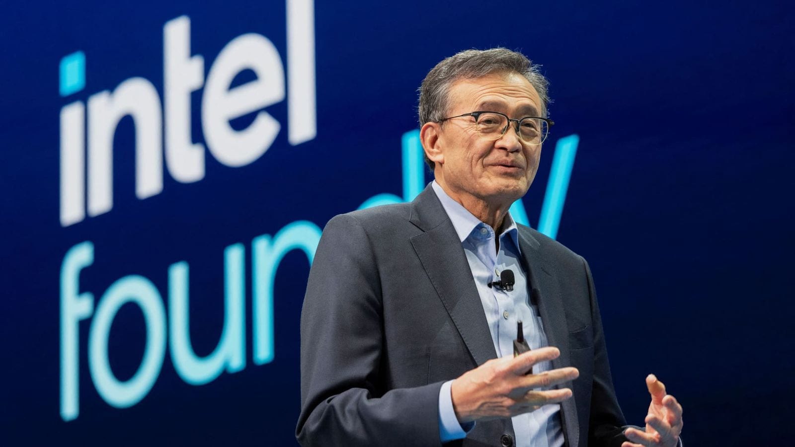
IBM expects partners Samsung, Intel, and Japan's Rapidus to commercialize the Nanostack technology over roughly the next five years — meaning production is expected around 2030. This is a research prototype, not a commercial product launch.
The Apple-Intel chip deal and Intel's own roadmap make Intel's role as a potential Nanostack licensee worth watching. Similarly, Samsung's HBM4 momentum shows how quickly Samsung can move from research to volume production when the architecture is ready.
What was IBM's last major chip technology advance?
IBM's previous chip manufacturing technology was introduced in 2021. The new Nanostack process can squeeze nearly twice as many transistors onto a chip as that 2021 generation, IBM said.
The New York Times reports that IBM says the new production process could keep chip innovation going for another 10 years. Industry analysts briefed on the announcement were described as impressed, while noting the approach will face competition.
Here's what we know so far: this is a research milestone, not a shipping product. The concrete next step is commercialization by Samsung, Intel, and Rapidus, with IBM targeting that window around 2030.
The broader race for AI compute efficiency — visible in moves like the SpaceX-Reflection AI compute deal and the Nvidia chip supply crunch — makes IBM's licensing model a meaningful input to how the next generation of AI hardware gets built.

0 Comments
Log in to comment
Not a member yet? Join the community
Pick a meme
KlipyHave a great take?
Drop your email — we'll send a magic link so you can post it. No password.
Not a member of the community? Join today.
Join the community →